Scaling down electronic components with diamond films
Diamonds are an engineer’s best friend. As well as their incredible hardness, diamonds have several physical properties that make them excellent for electrical devices – like light-emitting diodes (LEDs). One of the big challenges in electronics is continually trying to miniaturise devices: the smaller they become, the more heat is generated which reduces their lifespan, reliability, and efficiency. Effective thermal management is crucial. Dr Joana Mendes at the Instituto de Telecomunicações, Portugal, has reviewed how integrating diamond films with GaN high electron mobility transistors (HEMTs) can help achieve exactly that.
Diamond is a remarkable material – and not just for making jewellery. It’s so hard that only another diamond can cut through it. Diamond also possesses some remarkable thermal and electrical properties with extensive technological applications. These properties can be fine-tuned through selective doping (tweaking with other elements). It’s why Dr Joana Catarina Martins Mendes at the Instituto de Telecomunicações, Portugal, sees diamond as the future material for improving the performance of GaN (gallium nitride) high electron mobility transistor (HEMT) electronic devices.
An engineer’s best friend
A pure diamond is made entirely of carbon. At an atomic level, a diamond is simply a lattice of repeating carbon atoms with covalent bonds to their nearest four carbon neighbours. However, sometimes one of the carbons is replaced in the lattice by a non-carbon element known as a dopant.
When a dopant is introduced to a diamond, however, it may be a different size or have different electrical properties to the carbon atom it is replacing. While diamond is normally an exceptional electric insulator (blocking the flow of electric currents), some dopants can change its lattice shape on a molecular level and transform it into an excellent electrical conductor.

Diamond naturally has a fantastic ability to conduct heat: it’s the most-effective thermal conductor of all solid materials. This, combined with its potential for either excellent electrical conductivity or insulation, make it appealing for integration into electronic circuits for thermal management – particularly for highly compact or high-power devices.
But the smaller the device the higher the heat generated per unit of volume. Overheated devices are exponentially more likely to fail, and rising temperatures also decrease efficiency. So how can diamond help devices stay cool? Its highly effective combination of thermal conductivity and electrical insulation means that diamond could be used to extract heat from electronic devices.
Power LEDs
One of the challenges with using diamonds for technological applications is the price. Diamond mining is a tightly controlled market, and while natural gemstones may be sought after for their aesthetics, the predictability and customisability of lab-grown diamonds are highly appealing for scientific and engineering applications. Luckily, scientists have found a way to use very thin layers of artificial diamond to coat materials, improving its potential financial viability as a material for electronic devices.
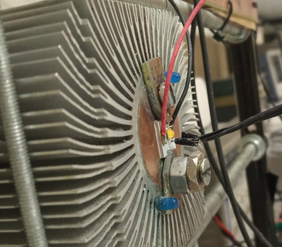
Mendes and her collaborators have reviewed the research on integrating diamond films into electrical circuits to make new high-power light-emitting diodes (LEDs) that have significantly longer device lifetimes. They found that taking advantage of the intrinsic properties of diamond – to replace the ceramic plate inside the LED package or even the board where the LED is assembled – helps achieve much better device performances.
Miniaturisation: thermal management
One of the electronics industry’s big drives has been finding ways to make components smaller. Moore’s Law, which predicts that the number of transistor components that will fit on a chip will double every two years, has overseen the explosive growth in computing power that has marked the last 60 years.
Consequently, transistors – the electrical components that can switch or amplify electrical signals – have been getting steadily smaller. In the 2020s, the thermal limits of how many transistors can be packed onto a single chip have started to be realised. This means that the heat load from having so many tiny components on a chip is so great that it essentially stops the device from working.

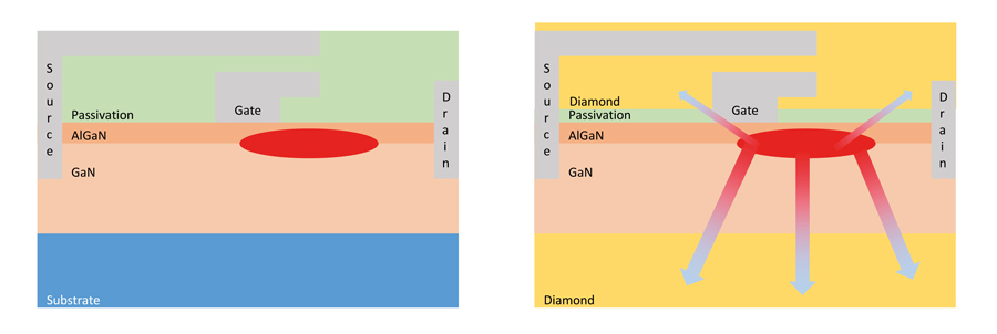
Mendes has been demonstrating that by changing the traditional materials inside the device package or even the board where the device is assembled to diamond, it is possible to regulate some of this high thermal load with the excellent thermal conductivity of diamond.
One device Mendes has been using diamonds for is LEDs. LEDs are highly sensitive to fluctuations in temperature as it affects both the colour of the light emitted and its intensity. For many applications, the stability of both properties is essential; Mendes has achieved this – and improved the lifetime and reliability of LEDs – with a diamond growth method to create thin diamond films that can be fashioned into devices.
Diamond films are typically grown in the lab using chemical vapour deposition. This method produces very high-quality thin films of many different materials, including diamond, and involves vapourising a series of precursor compounds that can then react or decompose on the surface of the substrate material to make the desired thin film. By changing the experimental conditions in chemical vapour deposition, it is possible to create thinner or thicker films and introduce dopants into the final material.
HEMTs are carefully designed to help electrons move through the device as quickly as possible.GaN HEMTs
With her success at improving the performance and lifetime of high-power LED components, Mendes has also been focusing on another area of device development for a type of transistor known as a high electron mobility transistor (HEMT).
HEMTs are a type of transistor usually fabricated from semiconductor materials like gallium nitride (GaN). What makes HEMTs so special is that they are carefully designed to help electrons move through the device as quickly as possible. In most semiconductors, electrons undergo collisions with the atoms and other electrons, reducing their overall mobility – but in HEMTs, the electrons can move faster and much more freely.

One of the advantages of having faster electrons is that the HEMTs can be turned on and off much more quickly. This produces transistors which are better and faster than other technologies.
However, while HEMTs have a better performance than standard transistors, heat generation is still a problem for creating long-lasting, reliable devices. Mendes reveals that it’s possible to create a better overall device by integrating diamond films with GaN HEMTs. GaN HEMTs are used in wireless communications, renewable energy generation, and many other applications; improving their performance and reliability with GaN-on-Diamond technology will likely have a significant impact.
Diamond films forever?
Despite its excellent performance, one of the biggest challenges of incorporating diamond into daily-life devices is that this increases the fabrication cost – going against the grain of the current practice of inbuilt obsolesce. However, there are applications where the lifetime of electronic components should be as long as possible – and as low weight as possible – such as space applications. Diamond films thus have significant potential in space electronics, helping to keep devices cool – and last longer.
Mendes and her team have been developing new methods to try and optimise the diamond deposition process to make it easier to create the types of films required for device integration and improve the cost efficiency of the process. Getting this manufacturing step right is an essential part of the future of these materials in electronic devices.
Personal Response
What are the limitations on diamond becoming part of all our electronic devices in the future?The ‘better – and cheaper – devices’ trend. Artificial diamond films are deposited from a mixture of methane and hydrogen – and the deposition of the material is not per se an expensive process. However, the integration of diamond films and electronic devices requires the development and optimisation of new processing lines and this is a costly procedure. LEDs, for instance, have become low-cost components. Are we (or the manufacturers) willing to trade low cost for higher efficiency and longer lifetime? The answer to this question will decide if, and when, daily-life electronic devices have an inner diamond core!