Electrode modification techniques for organic electronics
Organic electronics have become an increasingly popular way of making electronic devices and circuits. Traditionally, most electronics applications made use of metal-containing, or inorganic, chemical compounds such as silicon which are typically better for moving around the electronic charges that make up the electrical current in such circuits.

However, many organic molecules, that consist mostly of carbon and hydrogen atoms, can also be effective at conducting charges. The long chains of molecules, called polymers, that make up most plastics, can for example be modified using a dopant to make them as conductive as metal wires. The idea that organic compounds could be used as conductors or semiconductors, materials that only conduct charge under specific conditions, had such a significant impact that in 2000, Alan Heeger, Alan MacDiarmid and Hideki Shirakawa received the Nobel Prize in Chemistry for this work.
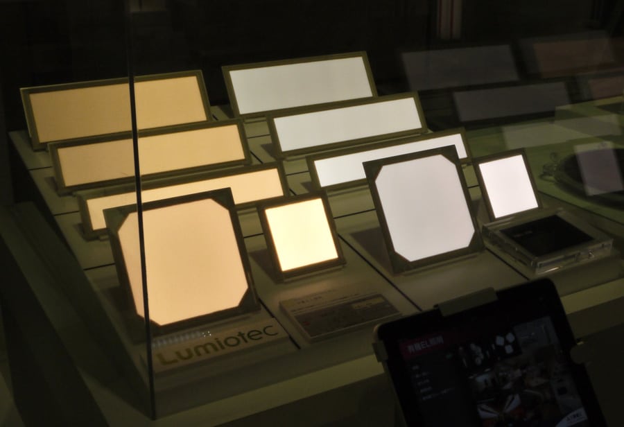
There are many reasons why organic electronics have become so popular. They can be lightweight, highly flexible and cheap to manufacture. Organic light emitting diodes (OLEDs) are one of the major success stories of organic electronics – OLEDs are now found in most of the displays we use and have made the possibility of a foldable mobile phone, first developed by Samsung, a reality. Furthermore, they can be used to make electronic paper, as the company Plastic Logic (Dresden, Germany) have shown using transistors (the type of small control switches which most modern technology is based on) made of organic semiconductors. And with steadily rising efficiencies, flexible organic solar cells integrated into bags or clothing will soon become a reality too.
Organic light emitting diodes (OLEDs) are one of the major success stories of organic electronics.
The three colleagues at Philipps-Universitaet Marburg are experts at finding new ways to improve how we make organic electronic devices. In particular, they develop novel strategies to improve the structural properties of organic semiconductors and their interfaces. They are using different characterisation techniques such as high-resolution microscopes, capable of imaging single molecules, X-ray diffraction and spectroscopy to really try and understand in detail the complex structures of the organic semiconductor materials and then use this information to improve their design.
Interfacing issues
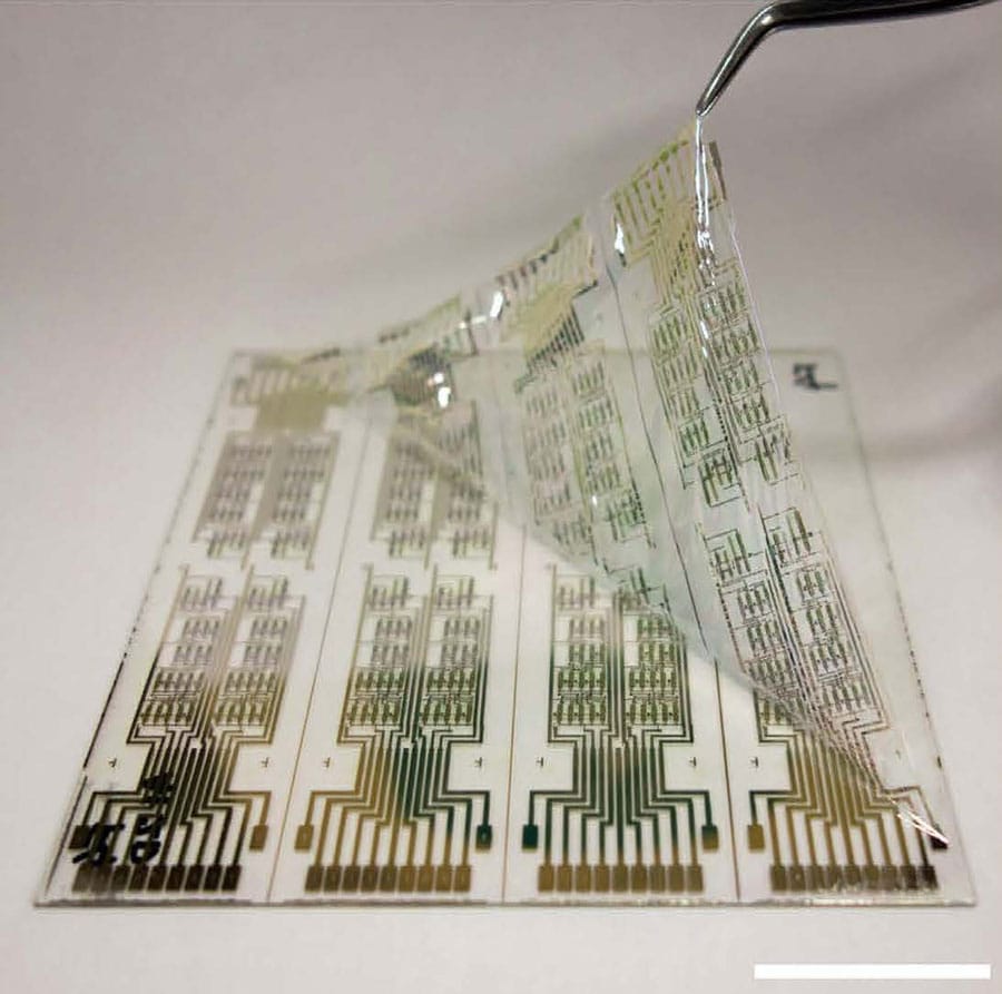
One area that the team has been focusing on is modification of the metal electrodes. One of the key issues in organic electronics lies at the interface between conventional metal electrodes and the novel organic semiconductor materials: the electrode acts as the charge injector for the organic semiconductor and the efficiency of this charge injection is very important for the overall efficiency of the device. The interface between the electrode and the semiconductor therefore is a crucial area to target for improving such devices. A useful measure in this context is the so-called work function difference between the metal and the organic semiconductor. Each has a material-specific work function value and the difference between the two is a measure for how easily charges can be transferred from one material to the other. The team at Marburg have recently shown that they can change the work function of metal electrodes in a controlled fashion by adding a single layer of molecules, a so-called monolayer, on top of the metal.
Control over the metal work function is important as this needs to be tailored for each organic semiconductor to make the most efficient devices. However, creation of these single organic monolayers is not easy. Usually these monolayers are applied in what is known as a wet chemical process which involves reactive solvents and is therefore difficult to incorporate into the fabrication of high-performance devices. The team at Marburg uses organic molecular beam deposition in ultra-high vacuum instead, which is more reliable, reproducible and suitable for the manufacture of complex devices. This method, like the competing wet chemical processes, has been used in the field for years, also to make work-function modifying monolayers. The team goes one step further in ensuring a precise control over their process and even correlates the molecular arrangement inside the formed films with the observed work function changes.
The Marburg team’s method uses organic molecular beam deposition, which is more reliable, reproducible and suitable for the manufacture of complex devices.
Organic molecular beam deposition
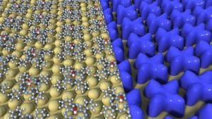
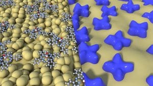
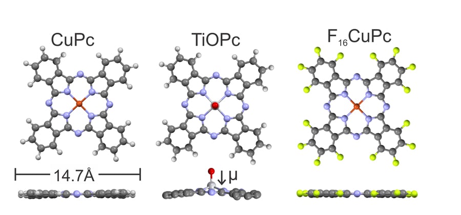
Organic molecular beam deposition works by heating the organic molecules to very high temperatures inside a vacuum chamber so that they form a vapour (this process is called sublimation). When brought into contact with the cold surface of the metal electrode, molecules adsorb and form a film on top of the metal. What the Marburg team then does is to heat the metal in order to remove any unwanted excess layers, until just the single desired monolayer is left. This means no harsh solvents are needed and there is excellent control over the process. Witte, Hauke and Widdascheck have shown this approach is highly successful for depositing layers of phthalocyanines, large molecules commonly used in organic electronics, onto metals such as silver, gold and copper. They have studied this both for idealised model surfaces, which can be used by theoretical physicists for detailed computational modelling, as well as for the less perfect surfaces of real device electrodes.
The flexibility of this approach means it is highly adaptable for different combinations of metal surface and organic semiconductor. Choosing different molecules for the monolayers or tuning the layer thickness allows to precisely enforce a specific work function value in the metal electrodes which is then compatible with a specific organic semiconductor or a specific organic device type.
Personal Response
Is organic molecular beam deposition scalable to mass produce such devices?
<> We certainly think so and so do the people at the company Heliatek (Dresden, Germany) who are one of the world’s leading R&D companies manufacturing efficient, large-area organic solar cell prototypes. The question you have to ask yourself is whether you want cheap devices with high throughput and low quality or whether you are after high-performance devices for sophisticated applications. In the latter case, OMBD is most likely your best option, since the cheaper solvent-based methods are less controllable and therefore less reproducible right now.