Architecting 3D integrated circuit fabrics at nanoscale
Dr Csaba Andras Moritz, entrepreneur and Professor of Electrical and Computer Engineering at the University of Massachusetts, Amherst, is developing a new nanoscale three-dimensional (3D) integrated circuit technology. This research has the potential to revolutionise the microelectronics industry with widespread socioeconomic impact.
2D Complementary Metal Oxide Semiconductor
The current two-dimensional (2D) Complementary Metal Oxide Semiconductor (CMOS) technology has been the cornerstone of integrated circuit design to date. It is used in the composition of all digital processors, graphics chips and the newly emerging Artificial Intelligence (AI) chips employed in computers, mobile phones and tablets, with applications in medicine, industry and space. Since its inception in the last century, 2D CMOS technology has remained a significant force of global socioeconomic progress; however, it is expected to reach its structural physical limits soon and will be unable to deliver the required advantages to new technologies. Until now, reducing the scale of CMOS integrated circuit (IC) architecture to provide smaller and more compact devices has driven the integrated circuit industry. Further scaling, however, is becoming more difficult. Scaling to sub-10nm technologies is proving to be very challenging due to the physical limitations of 2D CMOS technology. This is prohibiting future development. Current approaches to 3D have largely failed since they are based on monolithic stacking, and cannot provide the connectivity and efficiencies necessary for new applications.

A new direction
Professor Moritz and his collaborators are providing a new direction for the continuous miniaturisation of integrated circuits by switching to a fine-grain vertically-integrated 3D approach, based on an entirely new paradigm for CMOS. Instead of stacking, their model uses templates of vertical nanowires and connectivity between them to form circuits. Their work will enable the continuous scaling of integrated circuits, providing efficiency benefits such as an order of magnitude lower footprint, and reduced costs and energy consumption. The research team expect their research to stimulate developments in a variety of novel application domains.
Professor Moritz and his collaborators are providing a new direction
for the continuous miniaturisation of integrated circuits.
3D technology
Professor Moritz believes that three-dimensional technology could be extremely beneficial, particularly as achieving high degrees of connectivity is likely to become crucial for the advancement of future AI and microprocessors. Information integration theorists hypothesise that 3D connectivity is what enables the diversity and integration of the brain functions required for the emergence of consciousness.
Converting 2D CMOS into 3D is proving to be exceptionally difficult. Its customisation and manufacturing are not fundamentally compatible with fine-grain 3D integration. Assembling 2D CMOS layers into 3D in a monolithic layer-by-layer integration has shown to be of limited benefit.

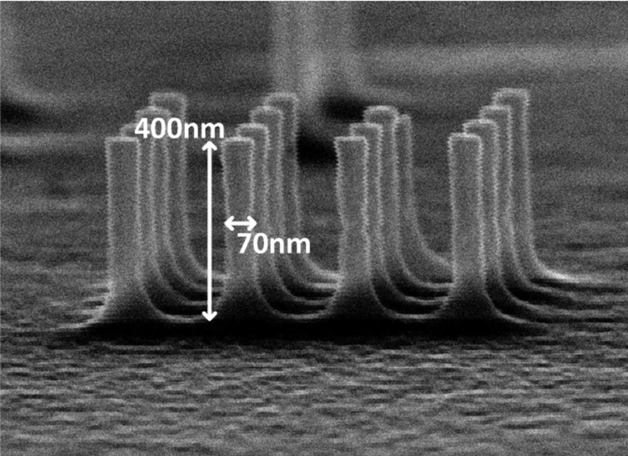
Rather than trying to adapt existing technology, Professor Moritz and his team are offering a brand new paradigm. They are developing a comprehensive 3D vertically integrated circuit fabric technology, Skybridge, the first fine-grained 3D CMOS integrated circuit technology. Core fabric aspects are developed concurrently achieving 3D compatibility. The researchers have designed nanostructures with vertical nanowires offering solutions built for connectivity and 3D heat management. They also propose a cross-layer approach combining device, circuit and manufacturability.
Where the layer-by-layer integration of 2D CMOS offered benefits of around 50%, Skybridge promises at least an order of magnitude efficiency improvement. This fine-grained 3D CMOS IC vertical assembly offers enhanced scaling capability and provides exceptional routability together with a connectivity reserved for future AI chips. Skybridge has recently been endorsed by several large semiconductor and CAD companies and, if adopted, could have a massive socioeconomic impact.

Skybridge Vertical-3D-CMOS
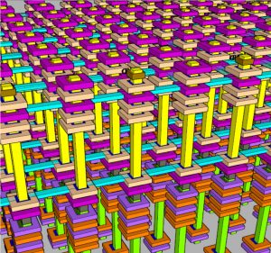
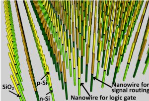
The research team are developing a novel vertical fine-grained 3D CMOS, based on Skybridge foundations, called Vertical-3D-CMOS (V3DC). They have devised a systematic method of building static CMOS circuits on a skeleton-style vertical nanowire structure. The circuits are all constructed on a homogenous vertical nanowire template. Pull-up and pull-down networks, made up of series and/or parallel connections are constructed. The series networks have active devices on a single nanowire, and the parallel networks are created by positioning and connecting active devices across several nanowires. A specially designed fabric component, called Vertical-Interlayer-Connection (V-ILC), allows the researchers to connect the pull-up and pull-down networks together in order to generate an output signal. They have developed additional V3DC fabric structures to allow both vertical and horizontal connectivity and a thermally-aware circuit synthesis. Working with leading CAD vendors, they support a largely commercially based suite of automated tools that have been able to generate and validate large V3DC Skybridge designs including a processor.

Preliminary evaluations
The research team have already carried out preliminary evaluations of this 3D nanofabric. Initial results show improvement in density of more than an order of magnitude compared to aggressively scaled CMOS with FinFETs and an improvement in performance/watt exceeding 16.5 times. The researchers’ projections promise further improvements over scaled CMOS, with potential for two orders of magnitude in very large-cale designs, assuming additional optimisations and CAD support.
This research has involved a detailed design of the core framework at nanoscale, specifying material choices and stipulating design rules, and building 3D V3DC circuit libraries and SRAM cells. The researchers have employed a bottom-up methodology, carried out a comprehensive evaluation including material considerations, nanocircuit and architecture-level designs, together with a variety of simulations. Experimental research has focused on the validation of fundamental fabric features. Electron beam lithography, which can draw customised patterns with sub-10 nm resolution, has been employed together with various manufacturing for etching and deposition, for experimental cleanroom demonstrations. The team also works closely with a leading provider of CMOS processes and equipment to develop a scalable manufacturing process deck for Skybridge. This includes using Process Explorer, an advanced tools suite from Synopsis, that was made available.

A system-level CAD tool
V3DC’s interconnections, device and circuit cell-layout design are significantly different from 2D CMOS, or stacked 3D, so the established CAD tools that are currently being used for design flow and evaluation are not appropriate for V3DC. To rectify this, Professor Moritz and his team have also developed a system-level CAD tool suite that enables the flow enabling validation of very large circuits such as microprocessors. This incorporates commercial CAD tools and enables benchmarking and validation of arbitrary complexity designs.
This project sets ambitious goals, but if this fabric is adopted it can revolutionise the microelectronics industry with far-reaching socioeconomic impact.
Ambitious goals
Professor Moritz remarks that “this project sets ambitious goals, but if this fabric is adopted it can revolutionise the microelectronics industry with far-reaching socioeconomic impact.” The research carried out by his team so far has shown that vertically-composed fine-grained 3D CMOS technology is crucial to finding 3D solutions that can extend far beyond CMOS, fuelling new technology. Industrial collaborators largely agree that there is no other 3D pathway showing as much potential. There has been remarkable growth in integrated electronics over the past two decades due to the scaling of CMOS. This research provides a scaling pathway that can be established at large-integration-scale for future ICs.

Dissemination
The research team also have several initiatives to disseminate their research results. A number of activities are in place to widen participation in computing and related disciplines at various academic levels as well as involving industrial participants. These include Think NanoPreneurshipTM, a platform for nanotechnology-based entrepreneurship. Professor Moritz aims to organise resources and facilitate experiences for undergraduate and graduate students of emerging VLSI, nanotechnology and nanoscience, as well as practitioners. This offers participants an appreciation of the business challenges that are specific to new nano-related ventures, and consequently better prepares them to work in and lead nanotechnology businesses.
Professor Moritz’s team, through his industrial and academic collaborators, place emphasis on a broad dissemination within the technical community. In addition to the publication of research papers, they have led special issues including in IEEE journals on 3D nanofabrics and lectured in IEEE VLSI, device and architecture forums.
Potential impact
This pioneering development of the Skybridge V3DC, in particular the increased connectivity and densities, could prove vital in new microprocessor architectures enabling increasing levels of complexity, which are not dominated by the interconnect delay factors of 2D CMOS. It can also be paramount in enabling AI designs with a much higher neuron density and layering than possible today. This approach will encourage research across many disciplines outside of the electrical and computing fields. The work of Professor Moritz and his team has the potential to support broad-ranging interdisciplinary research underpinned by CMOS technology; technology that has evolved for almost 50 years with widespread impact on STEM research.
Personal Response
What initially prompted your exploration of 3D nanoscale fabrics?
<> I have always been an entrepreneur and innovator at heart. Having followed the industry for decades, I noticed the reluctance to take on bigger vision type of projects. Industry does not often want to take the risk. Doing this type of project in academia is risky as well, as it requires a multidisciplinary mindset spanning material structures, device, circuit and architecture layers, often outside one’s comfort zone. Having brainstormed on new application requirements and possible pathways to realise them in the future, from both an academic and a commercial point-of-view, is what gradually crystallised the Skybridge 3D direction. We had a great experience with 2D CMOS as well as various nanoscale exotic fabric architecture directions and this seemed to be an opportunity, a new way to tackle an important problem that has high societal implications.