Probing surface morphology with virtual plasmonic dimers
The interaction of light (and, in general, electromagnetic radiation) with matter is at the core of a wide class of techniques frequently used to study the structure and dynamics of atoms inside molecules and bulk materials. For instance, in UV-vis spectroscopy, when visible light or ultraviolet radiation are absorbed by a molecule, electrons oscillate with characteristic frequencies that depend on the details of how the electrons are distributed within the molecule. Examining the absorption profile (or ‘absorption spectrum’), yields important information concerning the nature and distribution of chemical bonds between atoms. Whereas in isolated molecules light typically induces oscillations of only one (or a few) electrons for a given frequency, in systems like metal surfaces a large number of electrons can respond simultaneously to the radiation, and produce a collective oscillation, indicated as a surface plasmon resonance. A similar behaviour is also known to occur in metal nanoparticles. In this case, the radiation frequency at which the plasmon is observed is drastically affected by the dielectric medium supporting the nanoparticles. Dr Ingo Barke and his collaborators at the University of Rostock are pioneering methods to exploit the sensitivity of plasmon resonances in nanoparticles to develop ultrasensitive probes for surface structure determination.

Virtual plasmonic dimers
Dr Barke’s work focuses on small (~10 nm) silver atom clusters. He has shown that these nanoparticles exhibit unusual optical properties when they interact with silicon surfaces. In this case, even a single nanoparticle gives rise to two plasmon resonances, instead of the expected single one. A possible explanation of this intriguing observation is that the plasmon on the nanoparticle induces an ‘image dipole’ in the silicon surface, which oscillates at the same frequency as the nanoparticle plasmon. Effectively, a virtual ‘twin’ plasmon is created in the surface, which can couple with the nanoparticle plasmon and modify the optical properties of the nanoparticle. What makes this finding surprising, and, potentially, very far reaching, is that the surfaces considered in Dr Barke’s measurements belong to a material (crystalline silicon) that is semiconductive, rather than metallic. Whereas image dipoles are well-known in metals—in which conduction electrons are allowed to move freely between atoms in response to an external field—their appearance in a semiconductor surface is a very exotic phenomenon. Notably, the shape of the double resonance is extremely sensitive to the degree of coupling between the nanoparticle and the surface: a change in the effective nanoparticle-surface distance of less than one atom’s diameter is sufficient to affect the optical spectrum of the nanoparticle. This key finding prompted Dr Barke to explore the application of small nanoparticles to the ultrasensitive detection of geometric surface changes, for instance for the measurement of a film thickness at a surface and its spatial dependence.

Probing plasmon resonances with lasers
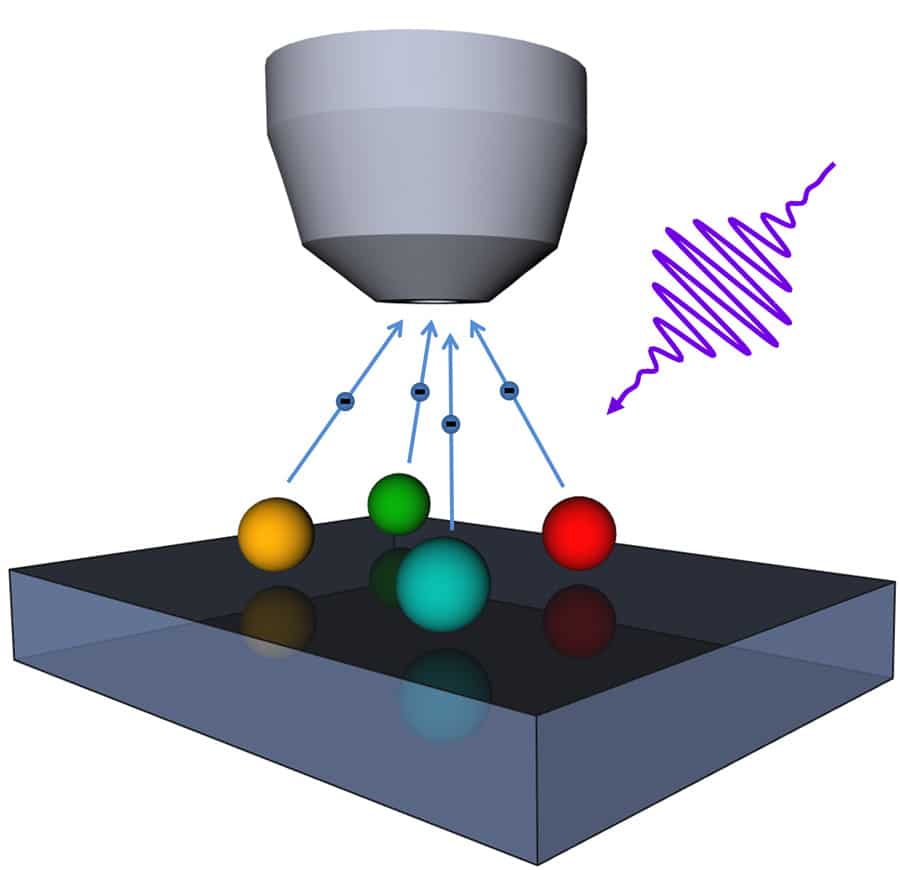
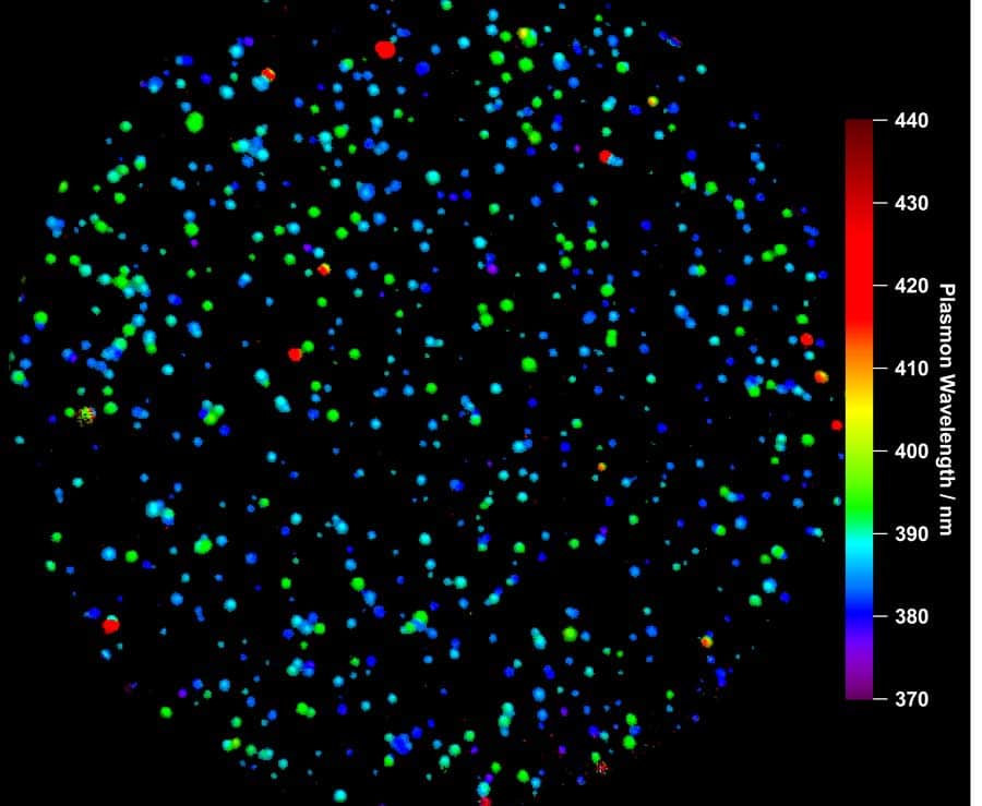
These advances in understanding the origin of virtual plasma resonances in nanoparticles have been made possible by an approach based on the combination of electron microscopy and optical excitation using lasers. This method, called photoemission electron microscopy (PEEM), achieves much higher resolutions than standard microscopy, making it possible to explore the spatial scales typical of few-atom clusters. Dr Barke’s team has pioneered the application of PEEM to the study of nanoparticle-surface interactions. In their approach, the laser radiation is tuned to span various colours (light frequencies) during the observation of the nanoparticles. In this way, the spectral properties of a large number of individual nanoparticles can be determined simultaneously. Different surfaces can then be compared, to work out statistically significant estimates of nanoparticle-surface couplings. This approach provides the basis for the validation of the virtual plasmonic dimer picture.
This opens up the possibility to control the behaviour of individual nanoparticles, especially in fundamental research.
Modelling plasmon coupling
A crucial component for understanding the underlying physics is the ability to model, using computational approaches, the influence of the detailed morphology and local geometry—particularly the distance between the nanoparticle plasmon and its surface counterpart—on the formation of multipole moments in the system. In nanoparticles, whose size is small compared to the excitation wavelength, the dipole approximation is typically used to understand how electrons move in response to the oscillating field of a perturbing radiation. In the present case it breaks down despite the small particle size because higher-order multipoles created by the interaction between particles and substrate become the key players and they are responsible for the observed changes in the optical properties of the nanoparticles near a silicon surface. The computational method developed by Dr Jean Lermé (University of Lyon, France) based on generalised Mie theory, and applied to the experimental results in collaboration with Dr Barke has made it possible to systematically explore how the variation of certain parameters at a subatomic scale (which is not achievable experimentally) affects the nanoparticle-surface coupling and to provide a solid quantitative basis for the plasmon dimer model.

Controlling nanoparticles with light
One of the main consequences of the virtual plasmon dimer model is that the properties of small (~10 nm) nanoparticles near a surface have to be treated individually, because the electronic coupling causing the appearance of the dimers and determining the plasmon energetics is strongly dependent on the detailed morphology and the local environment. This opens up the possibility of controlling the behaviour of individual nanoparticles, especially in fundamental research. For instance, the variation of the plasmon energies could be exploited to activate small subgroups of (or even individual) nanoparticles by tuning the wavelength of light precisely to the respective resonance energy. In this case, the nanoparticles could be used as far-field/near-field couplers, to create localised electronic excitations in host molecules adsorbed at desired locations on a surface. Another implication of Dr Barke’s research is that the high sensitivity of the plasmon response to the local environment could in principle be exploited to probe the nanoparticle surroundings, essentially at an atomic resolution. Provided the nanoparticle preparation and deposition are controlled accurately (for instance using self-assembly approaches) this can lead to the efficient and ultrasensitive detection of dielectric and geometric configurations at nanoparticle-surface interfaces. Technologically, this could have a large impact on the development of ultraprecise plasmonic rulers for the characterisation of thin spacer layers in semiconductor devices.