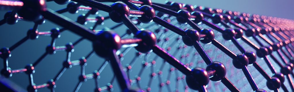
Tag: graphene
A new generation of wearable devices for telemedicine

Wearable gadgets such as smart watches, or wristbands, represent a user-friendly and cost-effective platform for the tracking of physiological parameters, such as heart rate and blood pulse oxygenation levels. However their rigid and opaque nature hinder the development of skin-conformable sensors that provide continuous and accurate data for telemedicine. Dr Emre Ozan Polat and his team from Kadir Has University […]
Read More… from A new generation of wearable devices for telemedicine
Caught on camera: Visual comprehension of chemical reactions
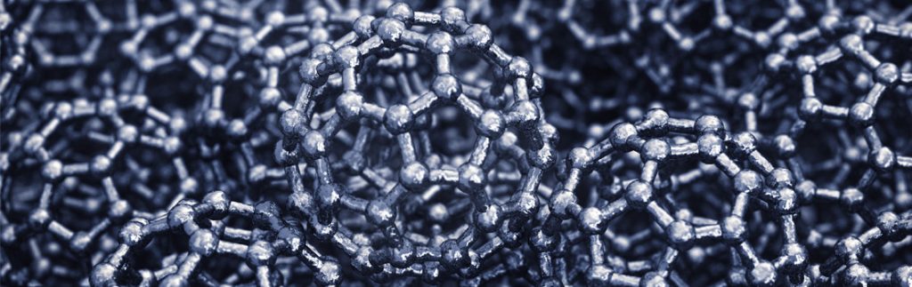
Using in-situ electron microscopy, Professor Dominik Lungerich at the Institute for Basic Science (IBS), Korea, and colleagues have produced a video of the assembly of a spherical all-carbon molecule, known as a buckyball, from a different planar molecule. Within this video, it is possible to see the precursor molecule morph into a buckyball as its bonds break and reform, providing […]
Read More… from Caught on camera: Visual comprehension of chemical reactions
Advanced chemiresistive materials for wireless sensor networks

When exposed to gases and vapours of certain chemicals in their surrounding environments, chemiresistive materials can change their electrical resistance, which makes them incredibly useful as sensors for air pollution. Through her work, Dr Esther Hontañón, a researcher at the Spanish Council of Research (CSIC) in Madrid, explores how the latest advances in materials science and 3D printing technology can […]
Read More… from Advanced chemiresistive materials for wireless sensor networks
Electron emission patterning: A new path towards smaller devices?
The demand for smaller and more powerful electronic devices is ever growing in many sectors of today’s society. Current technology limits how small devices can be. To develop smaller devices, new materials and manufacturing techniques are needed. Ali Aliev and Ray Baughman of the Alan G. MacDiarmid NanoTech Institute have developed a non-contact dry patterning technique for carbon nanotubes. Their […]
Read More… from Electron emission patterning: A new path towards smaller devices?